How ForwardEdge applied their unique honed expertise to conquer time.

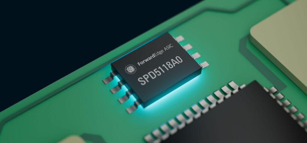
In 2023, ForwardEdge ASIC (FEASIC) was founded by Lockheed Martin to accelerate the development of best-in-class commercial and dual-use technologies essential to leading edge success. Our mission is to bolster domestic microelectronics capabilities and their enabling supply chains. ForwardEdge is an application-specific integrated circuit (ASIC) design center of excellence that will deliver best-in-class affordable microelectronics solutions. Our experienced, world-class workforce is a centralized hub of microelectronic and ASIC experts that are positioned to support a wide array of customers and missions.
The greatest enemy of high tech development is time. This is a story of how time was running out for a contractor, and they turned to ForwardEdge to solve a crippling mystery.
The mystery brought the project to a standstill
A key contractor on this project was facing a problem they could not identify, much less solve. After 10 months, gateware provided by a subcontractor still wasn’t working (even though they stated the original design was 100% complete and 80% verified) and time was running out. Key benchmark dates were approaching and failure was not an option (it never is). So they turned to ForwardEdge to evaluate the existing Verilog HDL (Hardware Description Language) RTL (Register Transfer Level) code.
Why ForwardEdge?
Five reasons: 25 years’ experience, vertically integrated ASIC and FPGA expertise from requirements to implementation, tight processes and methodology, and a cohesive team. In short, expertise in everything involved in ASIC development combined with processes to get it right the first time. “There is a huge advantage when you have an experienced team that can handle all aspects of ASIC in one place,” said FEASIC Senior Manager, Validation. “And the processes we have carefully developed over 25 years ensure we get it right the first time.”
Within 24 hours of examining the existing software and hardware architecture, including a background of the system interfaces, ForwardEdge had solved the mystery. It wasn’t just one problem – it was two rather serious issues, easily identified thanks to vertically integrated ASIC expertise. A “front end’ issue related to the hardware that connects the external “host” controller chips to the embedded processor, and a “back end” issue around software/firmware running on an embedded processor trying to access to the external storage media.
FEASIC first discovered issues on the software/firmware back end; the driver stack built into the Linux kernel did not support using legacy PCMCIA cards with modern access methods (memory mapped I/O) over parallel ATA. At the same time, the processing system in the FPGA did not support using legacy access methods (port mapped I/O). When attempting to boot the Linux kernel, this meant that the PCMCIA card was not recognized.
As for the front end RTL issue:
-
- At a basic level, numerous mistakes in naming and connection that would render the design non-functional.
- The logic was not designed correctly for the required interfaces (AXI and external chip-specific interfaces).
- Finite State Machines (FSM) sequencing and timing was incorrect related to the operational specifications.
- Incorrect handshake logic that would cause the design to hang.
- No clock-crossing logic between different clock domains of the design.
- No error detection or response logic.
- No design documentation.
- Verification testbench only attempted to verify one part of the design on its own (i.e., “in a vacuum”) and had the same design flaws as the RTL code.
Problems identified. Now – how to fix them?
Within one day of receiving the request to re-design the existing logic, FEASIC outlined a 30-day plan and a list of deliverables.
Front end:
-
-
- Complete redesign of the architecture.
- Complete recode and delivery of the RTL from the ground up (no reuse of existing logic).
- Testbench creation and verification of the new logic.
- Complete Design Specification for the delivered design.
- FPGA (Field Programmable Gate Array) design and integration support related to the provided RTL design.
-
Back end:
-
-
- Debug PCB (Printed Circuit Board) setup to have reproducible error.
- Implement automated build process to accelerate test iterations.
- Resolve AXI slave error that enabled and discovered patapcmia (device driver) was not being compiled correctly.
- Investigate device interrupt handling options.
- Develop device drivers rely on polling methodology to mask out interrupt error handling.
-
It did not take 30 days. “We delivered design, verification and documentation 4-days ahead of schedule,” stated FEASIC Senior Logic Design Manager. “Once we identified the problems, we quickly delivered a solution, the customer happily approved it and the project advanced to completion.”
Reach the leading edge with confidence
Development on the leading edge involves many challenges, so having the confidence that you can conquer these challenges and deliver solutions quickly and efficiently is vital. You can be sure of ForwardEdge. Sure of our technology, quality, processes and methodologies, speed and reliability of our vertically integrated approach to developing ASICs.
Get the ForwardEdge
To work with ForwardEdge for your program’s microelectronics and ASIC needs, just reach out.